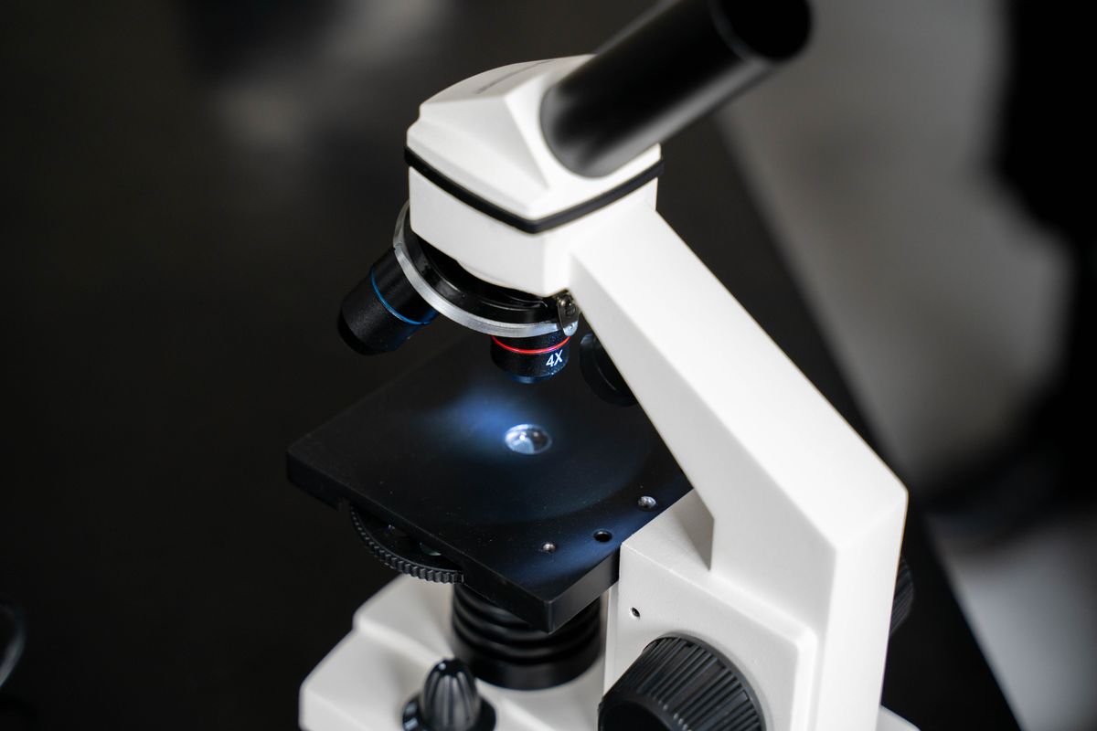
An electron microscope works by firing a focused beam of electrons at a sample and detecting how those electrons interact with it. Because electrons have a much shorter wavelength than visible light — roughly 100,000 times shorter — they can reveal details far too small for any light microscope to see. Modern electron microscopes can resolve features as small as 0.1 nanometres, which is smaller than a single atom.
Picture a light microscope: you shine light through or onto a specimen, glass lenses magnify the image, and your eye or a camera captures it. Now replace the light bulb with an electron gun, replace the glass lenses with electromagnetic coils, replace the air inside with a vacuum, and replace your eye with a phosphor screen or electronic detector. That is an electron microscope. Instead of photons, it uses electrons. Instead of magnification by bending light, it magnifies by scanning or transmitting a beam of electrons through magnetic fields.
Here is how the whole thing works, from the electron gun to the final image, covering both SEM and TEM.
How an Electron Microscope Works: The Basic Principle
Every electron microscope — whether scanning (SEM) or transmission (TEM) — operates on the same core principle. A stream of electrons is generated, accelerated, focused, directed at a sample, and the resulting signals are converted into an image.

The process follows five steps:
- Electron generation. An electron source, usually a heated tungsten filament or a field emission gun, emits electrons.
- Acceleration. The electrons are accelerated to high energies — typically 5 to 300 kiloelectronvolts (keV) — using a high-voltage electric field. Higher voltages give shorter wavelengths and better resolution.
- Beam shaping. Electromagnetic lenses (actually coils of wire that generate magnetic fields) focus the electrons into a narrow beam. These are not glass lenses — they are magnetic fields that bend the path of charged electrons, just like a glass lens bends light.
- Sample interaction. The focused beam strikes the sample. The way electrons interact with the material determines what kind of image is produced.
- Signal detection. Detectors capture the resulting signals — transmitted electrons, secondary electrons, backscattered electrons, or X-rays — and convert them into an electronic image displayed on a screen.
A vacuum pump maintains the entire column at low pressure. Without vacuum, air molecules would scatter the electron beam, reducing resolution and damaging the electron source.
TEM: Transmission Electron Microscope
A transmission electron microscope works by passing electrons through an ultra-thin sample and forming an image from the electrons that make it through.
Here is how it works. The electron beam is focused by condenser lenses to a broad, parallel beam that illuminates the sample. The sample must be extremely thin — typically less than 100 nanometres — because electrons need to pass through it. Thicker regions absorb or scatter more electrons, creating darker areas in the image; thinner regions let more through, creating brighter areas. This is called "mass-thickness contrast."
After passing through the sample, the beam enters the objective lens — the most important lens in a TEM. It forms the first magnified image, which is then further magnified by intermediate and projector lenses before hitting a phosphor screen or a CCD camera. The final magnification can reach 50 million times, enough to image individual atoms.
Key facts about TEM:
- Resolution: 0.1 nm or better (atomic scale)
- Magnification: up to 50 million×
- Sample thickness: less than 100 nm
- Image type: 2D projection of internal structure
- Electron energy: 60–300 keV (higher for thicker samples)
TEM is used to study the internal structure of materials: crystal lattices, dislocations in metals, virus particles, nanoparticles, and the internal organisation of cells. It was the first type of electron microscope, built by Ernst Ruska in 1931 — work that earned him the Nobel Prize in Physics in 1986.
SEM: Scanning Electron Microscope
A scanning electron microscope works differently. Instead of passing electrons through the sample, it scans a finely focused electron beam across the surface and detects electrons that are knocked off.
The beam is focused to a fine point — as small as 1 nm in diameter — and scanned in a rectangular raster pattern across the sample, line by line, pixel by pixel. This is similar to how an old CRT television paints an image. At each point, the beam interacts with the sample, and detectors collect the signals.
The most common signals used in SEM are:
- Secondary electrons: Low-energy electrons ejected from the sample surface. They reveal topography — the texture and shape of the surface — producing the detailed, 3D-looking images that SEM is famous for.
- Backscattered electrons: Higher-energy electrons that bounce off deeper within the sample. They reveal compositional contrast: heavier elements appear brighter because they scatter more electrons.
The detectors feed their signals to a computer that builds the image pixel by pixel, synchronised with the beam position on the sample. The result is a black-and-white image with exceptional depth of field — far better than any light microscope.
Key facts about SEM:
- Resolution: 1–10 nm (surface features)
- Magnification: up to 2 million×
- Sample requirements: must be electrically conductive (non-conductors get a thin gold or carbon coating)
- Image type: 3D-like surface topography
- Electron energy: 1–30 keV
SEM is used for surface analysis of materials: fracture surfaces, integrated circuits, pollen grains, dust particles, biological tissues, and forensic evidence. Because sample preparation is simpler than TEM, SEM is more widely used in industry.
SEM vs TEM: A Comparison
| Feature | SEM | TEM |
|---|---|---|
| What it images | Surface | Internal structure |
| Beam type | Focused spot, scanned | Broad parallel beam |
| Sample thickness | Any (bulk) | <100 nm |
| Resolution | 1–10 nm | 0.1 nm (atomic) |
| Max magnification | ~2,000,000× | ~50,000,000× |
| Sample prep | Coating for non-conductors | Thin sectioning + staining |
| Image appearance | 3D-like surface | 2D projection |
| Electron energy | 1–30 keV | 60–300 keV |
| Typical cost | $50k–$500k | $100k–$5M |
| Common uses | Materials, QC, forensics | Biology, nanomaterials, crystallography |
Both techniques are often complementary. A researcher might use SEM to examine surface defects on a metal fracture, then use TEM to study the crystal structure beneath the surface.
Sample Preparation for Electron Microscopy
Sample preparation is one of the most critical aspects of electron microscopy. A poorly prepared sample produces poor images regardless of the microscope quality.
For SEM: Samples must be dry, stable in vacuum, and electrically conductive. Non-conductive samples (most biological tissues, polymers, ceramics) are coated with a thin layer of gold, platinum, or carbon — typically 5–20 nm thick — using a sputter coater. This prevents charging, where the electron beam builds up static electricity that distorts the image. Biological samples are usually chemically fixed, dehydrated, dried at a critical point, and then coated.
For TEM: Samples must be thin enough for electrons to pass through — under 100 nm. This requires specialised techniques:
- Ultramicrotomy: A diamond knife cuts sections thinner than 100 nm from a resin-embedded sample.
- FIB (Focused Ion Beam): A beam of gallium ions mills away material to create thin lamellae, used primarily for semiconductor and materials samples.
- Negative staining: Heavy metal salts (uranyl acetate, phosphotungstic acid) are applied to give contrast around small particles like viruses.
- Cryo-EM: Samples are flash-frozen in liquid ethane at -196 °C, preserving them in a native, unstained state — a technique that won the 2017 Nobel Prize in Chemistry.
Common Misconception: Electron Microscopes Are Just Powerful Light Microscopes
A common misconception is that an electron microscope is simply a light microscope with higher magnification — as if you could just turn up a dial on an optical microscope and see atoms. That is not how it works.
Electron microscopes do not use light at all. They use electrons, and the entire imaging process is fundamentally different. The resolution limit of a light microscope is set by the wavelength of visible light — about 200 nm (the Abbe diffraction limit). No amount of lens improvement can beat this. An electron microscope beats it by replacing photons with electrons, which have a wavelength of about 0.0025 nm at 200 keV — roughly 100,000 times shorter.
This is why the electron microscope was invented in the first place. Physicists knew in the 1920s that the resolution of light microscopes had hit a wall. Louis de Broglie showed in 1924 that electrons have wave-like properties with extremely short wavelengths. Ernst Ruska built the first electron microscope in 1931 to exploit this, and the field of microscopy was transformed overnight.
For the fundamentals of how optical microscopes work, see how does a microscope work. The lenses in both types of microscope serve the same purpose — focusing radiation — but the lens refraction guide explains how glass lenses bend light, while electron microscopes use magnetic fields to bend electron beams.
External Resources
- VA Diagnostic EM: What Is an Electron Microscope and How Does It Work? — clear overview of EM principles, instrumentation, and clinical applications
- TESCAN: Electron Microscopy Fundamentals — SEM, TEM & STEM — illustrated guide to how each electron microscopy mode works
- Technology Networks: SEM vs TEM — direct comparison of scanning and transmission electron microscopy techniques
For the broader story of how microscopy advanced from the first lenses to atomic-scale imaging, see our optical fibre invention article for another story of physics pushing past apparent limits. And for the optical counterpart, total internal reflection explains the waveguide physics that guides light — analogous to how magnetic lenses guide electrons.
Frequently Asked Questions
How does an electron microscope work in simple terms?
An electron microscope works by firing a beam of electrons at a sample and detecting how those electrons interact with it. Electrons have a much shorter wavelength than visible light, so they can reveal details thousands of times smaller than a light microscope can see. Electromagnetic lenses focus the beam, and detectors convert the electron signals into an image on a screen.
What is the difference between SEM and TEM?
SEM (Scanning Electron Microscope) scans a focused electron beam across the surface of a sample to create a 3D image of its surface, with magnification up to 2 million×. TEM (Transmission Electron Microscope) passes electrons through an ultra-thin sample to reveal internal structure, with magnification up to 50 million×. SEM shows surfaces; TEM shows interiors.
Why do electron microscopes need a vacuum?
Electron microscopes require a vacuum because air molecules would scatter the electron beam before it reaches the sample. The vacuum allows electrons to travel in a straight line from source to sample to detector, preserving image sharpness. It also prevents contamination of the electron source and reduces background noise.
Can electron microscopes see atoms?
Yes. Modern transmission electron microscopes (TEMs) can resolve individual atoms. Aberration-corrected TEMs achieve sub-angstrom resolution — below 0.1 nanometres — which is smaller than the diameter of most atoms. Scanning electron microscopes typically reach about 1 nm resolution, enough to see large molecules but not individual atoms.
How is an electron microscope different from a light microscope?
A light microscope uses visible light and glass lenses; an electron microscope uses electrons and electromagnetic lenses. Electron microscopes have much higher resolution (0.1 nm vs 200 nm for light microscopes) and magnification (up to 50 million× vs 2000×). However, electron microscopes are far more expensive, require vacuum, and need extensive sample preparation.
What are the main components of an electron microscope?
The main components are: (1) an electron source or gun that emits electrons, (2) electromagnetic condenser lenses that focus the beam, (3) an objective lens for fine focusing, (4) apertures that control beam size, (5) a sample stage, (6) detectors that collect signals, and (7) a vacuum system. The entire column from source to detector is kept under high vacuum.

About Umar Farooq
Umar Farooq writes in-depth guides on the physics of light and optics — from reflection, refraction, and lenses to diffraction, lasers, and fiber optics, explained from first principles.
Read more about Umar Farooq →